Designing Custom Triggering Applications with the LabVIEW FPGA Module
Overview
One of the primary applications of reconfigurable hardware based on RIOTM Technology is the ability to create custom hardware triggering conditions. Using the LabVIEW FPGA Module along with any RIO-enabled hardware, you can quickly and easily create customized hardware. When building applications using these products, there are several considerations to keep in mind. This document outlines the creation of a custom triggering application and discusses best practices for creating scalable, maintainable, and robust FPGA code with LabVIEW. The example program Custom Triggering with the LabVIEW FPGA Module is included with this application note.
Contents
- Introduction to LabVIEW FPGA and RIO Technology
- Defining the Customer Hardware with the LabVIEW FPGA Module
- Creating the Application Programming Interface
- Conclusion
- Additional Information
Introduction to LabVIEW FPGA and RIO Technology
NI is the driving force behind the concept of virtual instrumentation. Virtual instrumentation harnesses the power of the PC and commercial-off-the-shelf hardware to create configurable, user-defined instrumentation systems based on intuitive, graphical software. It gives engineers and scientists the capability to build measurement and automation systems that suit their specific needs instead of being limited by traditional fixed-function, vendor-defined instruments. A simple example of this would be using LabVIEW application software and a plug-in data acquisition device to create a custom system with similar functionality of a traditional oscilloscope, DMM, and event counter all at once. With the LabVIEW FPGA Module and RIO-enabled hardware, NI has extended the concept of virtual instrumentation to provide engineers and scientists with the flexibility to define the functionality of the data acquisition device itself. Scientists and engineers can now use LabVIEW graphical programming to create user-defined custom hardware, providing cost and flexibility benefits over the vendor-defined hardware typically used in a virtual instrumentation system.
An FPGA (field-programmable gate array) is a semiconductor which contains a large number of disconnected logic gates. Programming an FPGA often requires low-level EDA software that defines logic functions by connecting the gates, thus creating a customized processor and in turn customized hardware. The LabVIEW FPGA Module allows engineers and scientists to easily create custom hardware graphically, without needing to learn low-level EDA tools. Furthermore, because an FPGA does not have a fixed hardware structure, the connections can be reprogrammed. Every time you compile your LabVIEW code to the FPGA target you create a new custom hardware, thus allowing for reconfigurable input and output (RIO) enabled hardware.
NI offers a family of RIO enabled hardware targets, including PCI and PXI data acquisition devices, the Compact Vision System, and CompactRIO. CompactRIO delivers the power and flexibility of RIO in a highly rugged enclosure. This paper will discuss how to create a custom triggering application using CompactRIO, the LabVIEW FPGA Module, and the LabVIEW Real-Time Module. Triggering is a common function of most plug-in data acquisition devices and is often used to start and stop acquisitions. In this application, we will define the triggering logic on the RIO target ourselves and then integrate our custom hardware with a host LabVIEW application. It is important to understand that creating custom RIO applications is a two-fold process. The first step is to configure the RIO hardware using the LabVIEW FPGA Module. The next step is to create a driver API for your hardware using LabVIEW for Windows or the LabVIEW Real-Time Module. Once a high-level API is created, a programmer will have readable and usable code available to program a virtual instrument.
Defining the Customer Hardware with the LabVIEW FPGA Module
Typically, FPGAs are configured using low-level software development tools such as VHDL or Verilog. The LabVIEW FPGA Module presents a high-level, graphical model for synthesizing FPGAs. Since the LabVIEW FPGA Module is an extension of LabVIEW for Windows, you get the benefits of rapid development that is provided by an intuitive programming tool that is similar to flowcharting. The palette shown when targeting a RIO device from LabVIEW is a subset of the LabVIEW for Windows functions palette. This set of functions consists of only those functions that you can use to be synthesized in the fixed-point structure of an FPGA.
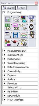
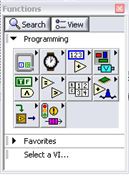
LV Palette FPGA Palette
Figure 1. LabVIEW Function Palettes
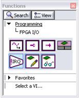
Although all RIO enabled hardware supports custom triggering, we will discuss this specific application developed for CompactRIO. We will create three triggers to trigger on an analog edge, digital edge, or analog window . We define these triggers by directly monitoring the acquired analog and digital signals on the channels of our CompactRIO digital and analog modules. These channels are accessed using the I/O functions found on the FPGA I/O palette shown in Figure 2.
Figure 2. FPGA I/O Palette
To use the Device I/O functions, simply place an FPGA I/O Node on the block diagram and left-click the function to view the I/O already added to the project, or to add new input and output. Figure 3 shows the New FPGA I/O dialog box.
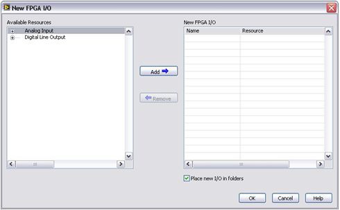
Figure 3. New FPGA I/O Dialog Box
Figure 4 shows the block diagram of the analog edge trigger used in the AnalogEdge subVI. The block diagram consists of a sequence structure with two sequences. The first sequence contains triggering logic for a "Rising" or "Falling" edge analog trigger. We are showing the case for the "Falling" edge case below. The loop polls the analog value of the channel as quickly as the hardware module can return data using the FPGA I/O Node. With each loop iteration we compare the current acquired value with the value obtained from the previous loop iteration to the trigger level. The trigger level was defined by the user with the Trigger Level control. If the acquired value is less than the trigger level and the previous value is greater than the trigger level, the trigger has fired and a value of “true” is sent to the stop condition of the While Loop. The While Loop will also stop if the timeout expires. The “Rising” edge case is similar but is looking for a rising analog edge instead of a falling analog edge.
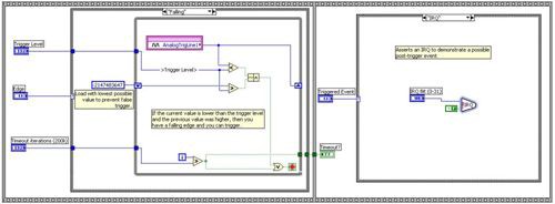
Figure 4. Block Diagram of AnalogEdge VI
When the loop stops, the program will proceed to the next sequence to execute the post-trigger event. In our example, the user can select between None or IRQ. If the user selects IRQ, an interrupt will be asserted on the interrupt line of the FPGA device that the user has selected with the IRQ bit (0-31) control. A programmer is not limited to the post trigger options we have utilized, but could write any code desired for the post trigger event such as generating a pulse train, acquiring analog data, setting digital lines high or low, etc. We also pass a Boolean value to the Timeout? indicator to specify if post-trigger event occurred due to a trigger or a timeout.
Now that we have defined our analog edge trigger in the AnalogEdge subVI, we can use that subVI in our top-level LabVIEW FPGA VI, TriggerDemo VI. The TriggerDemoVI will contain subVIs for each triggering case (AnalogEdge VI, AnalogWindow VI, and DigitalEdge VI). The AnalogWindow and DigitalEdge subVIs will be built similarly to the AnalogEdge VI, but with different I/O functions and different logic specific to that trigger type. All of our triggering subVIs must be placed into one main VI because only one VI can be compiled to the FPGA. It was not necessary to use subVIs, but we made use of them in this example because they are a great way to encapsulate and modularize your code.
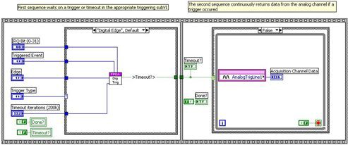
Figure 5. Block Diagram of the TriggerDemo VI
Figure 5 shows the block diagram for the TriggerDemo VI. Like the subVIs we created, it also consists of a sequence structure with two sequences. The first sequence uses a case structure to determine what type of triggering the user has selected in the “Trigger Type” control and then calls the appropriate subVI. A new trigger type could easily be inserted by simply adding a new value to the Trigger Type enum, adding a new case in the Case structure, and creating a new subVI for that trigger type. The VI remains in the first sequence until the triggering subVI completes, either by receiving a trigger or timing out. The VI then proceeds to the second sequence. The second sequence uses a Case structure to determine if a timeout has occurred or if a trigger has fired. If a timeout has not occurred, a trigger has fired and we begin an analog input acquisition.
Now that we have one top-level VI, we are ready to compile our VI for the RIO-enabled device. In this example, we are using the CompactRIO cRIO-9102. The front panel controls and indicators represent registers in the FPGA that can be written to or read from a host application. Once the LabVIEW FPGA code is compiled and downloaded to the RIO hardware, we can integrate that hardware with a LabVIEW Real-Time Module application.
Creating the Application Programming Interface
The second component of any LabVIEW FPGA application is to create an Application Programming Interface (API) for the FPGA VI. In the LabVIEW Real-Time Module (or LabVIEW for Windows), there is a small set of functions that you use to access the FPGA: Open FPGA Reference, Read/Write Control, Invoke Method, and Close FPGA Reference. These functions provide all of the necessary control over the FPGA, such downloading, reading or writing data, and starting or stopping hardware execution. Integrating an FPGA VI into an application using these functions alone, however, can make your application hard to read, hard to scale, and hard to maintain. Using these low-level functions as building blocks, however, you can create a set of subVIs which can function as an easier-to-use high-level API for use on your host.
There are several benefits to creating an API for your LabVIEW FPGA code. One major benefit that an API provides is abstraction, which involves grouping low-level code into logical functions or data stores. For example, one of the first things to do in an application is initialize your software and hardware. The process of initialization may be several steps of low-level code, but can be easily grouped into one subVI:
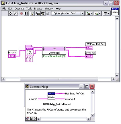
Figure 6. Abstraction of the Initialize Function in the FPGATrig_Initialize VI Block Diagram
Creating the API greatly increases the usability of your FPGA VI by hiding the low-level functionality and increasing modularity of the code. Once the subVIs are created, you can simply place them into any LabVIEW Real-Time or LabVIEW for Windows application as functional nodes. In our example, we have created 5 subVIs shown in Figure 7: Initialize, Triggering, Start, Read, and Clear.
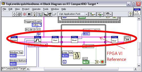
Figure 7. Block Diagram of TopLevelAcquisitionDemo VI
Each subVI performs one function and together they form an easy to read and maintain application. Documentation is also easier in the example above. Using good icons and VI documentation in an API greatly improves the readability of the code. Refer to the LabVIEW Help to learn how to create icons and document VIs.
There are several architectural considerations when creating an API. It is good LabVIEW programming architecture to have three main components to any application: Open or Initialize, Operations (Reading or Writing), and Close. For the FPGA Trigger Demo example, we have created this architecture by making an initialize VI, three ‘operations’ VIs, and a Clear VI. The glue that binds each subVI together is the FPGA VI Reference, which is obtained from the Open FPGA Reference function. You can pass this reference into and out of subVIs to create an easy-to-use interface that matches many other common LabVIEW APIs, such as DAQmx, File I/O, Report Generation, etc. In order to keep the FPGA VI Reference consistent amoung subVIs, bind the output of the Open FPGA Reference to a type definition and use this type definition in the subVIs. Another key component to an API is good error handling. By passing the error cluster from one subVI to the next, you make your program more robust and add data dependency between subVIs.
There are several points to highlight in the FPGA Trigger Demo example. In the Initialize VI (FPGATrig_Initialize VI), we call the Open FPGA Reference and the Invoke Method functions to obtain a reference to the VI and to ensure that the FPGA VI is downloaded to the target. The Triggering VI (FPGATrig_PolymorphicTrigger VI) is a polymorphic VI which calls one of the three individual triggering cases depending on the type of triggering desired (FPGATrig_DigitalTrigger VI, FPGATrig_AnalogEdgeTrigger VI, and FPGATrig_AnalogWindowTrigger VI). Each of these triggering VIs on the host configures the triggering application on the FPGA, by reading and writing to the FPGA registers using the Read/Write Control function as shown in Figure 8. The remaining two triggering methods are identical to Figure 8, only the control values are different for each triggering type.
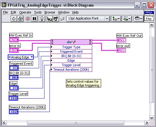
Figure 8. Block Diagram of FPGATrig_AnalogEdgeTrigger VI
The Start VI (FPGATrig_Start VI) simply runs the FPGA VI when it is called by the Run method. Once the VI is running, the Read VI (FPGATrig_Read VI) is called inside of a loop to read the data from an analog input module. The Read VI waits for the trigger, checks for a timeout, and then outputs the data to the TopLevelAcquisitionDemo VI. Another important feature of the Read VI is that it generates an error if there is a timeout. Finally, the Clear VI (FPGATrig_Clear VI) aborts the FPGA VI and calls the Close FPGA Reference function.
With a well thought out and executed API, a programmer can create ‘toolkits’ for their FPGA VIs that can be easily implemented into several larger programs.
Conclusion
The LabVIEW FPGA Module and CompactRIO hardware can be used to easily create custom hardware. This user-defined hardware gives the developer full control to customize hardware necessary for their application. Once the custom hardware has been created, it can be integrated with a LabVIEW Real-Time or LabVIEW for Windows application. For maximum maintainability, readability, and scalability, creating custom hardware with LabVIEW FPGA should always be a two-part process. First, create the code to define FPGA hardware, and second, create an Application Programming Interface to access the RIO device.